
A2Z EMS PCB Assembly
U.S.-based turnkey PCB assembly for startups & hardware team
Looking for dependable manufacturing support? This blog explains how PCB assembly services improve production consistency, reduce delays, and support both prototype and full-scale builds. Learn practical insights on pcb assembly process and managing pcb assembly costs effectively for better results. A2Z EMS shares real-world manufacturing perspectives that can help you make smarter decisions.
👉 Read the full blog and explore how to improve your PCB production strategy.
https://www.a2zems.com/post/why-choose-a2z-electronics-for-pcb-assembly-services-in-illinois

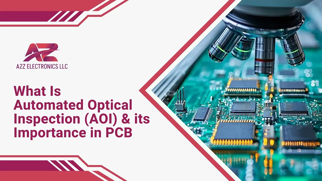
In modern electronics manufacturing, precision is non-negotiable. Even a slightly misplaced resistor or an imperfect solder joint can prevent a product from functioning properly. That’s where automated optical inspection becomes essential. It enables manufacturers to detect defects early—before they turn into expensive production failures.
By 2026, the global automated optical inspection systems market is expected to surpass $1.6 billion. As the demand for faster, more accurate PCB inspection continues to grow, advanced AOI systems are becoming indispensable in high-reliability production environments.
This guide explores what automated optical inspection is, how it works, and why it plays a vital role in today’s PCB assembly workflows.
Let’s begin with the fundamentals: what is AOI?
AOI stands for automated optical inspection. It is a visual inspection method that uses high-resolution cameras and specialized software to examine a printed circuit board for manufacturing defects. These defects may include missing components, soldering errors, polarity mistakes, or alignment inconsistencies.
The core AOI meaning is straightforward: inspect circuit boards quickly and accurately while eliminating the variability of manual inspection. A typical AOI machine scans the board and compares captured images against reference data or design files. Any deviation is automatically flagged for review.
This technology plays a critical role in maintaining quality standards in PCB AOI environments.
How Does Automated Optical Inspection Work?
A standard optical inspection system follows a structured process:
The PCB is positioned under calibrated lighting.
Cameras capture high-resolution images.
Inspection software analyzes and compares images to reference data.
Any inconsistencies are highlighted for operator review.
Some AOI systems rely on 2D imaging, while advanced models use 3D measurement to analyze component height and solder volume. This capability allows detection of subtle issues such as insufficient solder or lifted leads. The inspection process is fast, precise, and well-suited for modern SMT production lines.
Why AOI Is Important in PCB Assembly and Manufacturing?
Manual inspection methods are time-consuming and inconsistent. As PCB designs become more complex and production cycles shorten, manual processes alone are no longer sufficient.
Automated optical inspection PCB setups offer several advantages:
Detect defects early in the production cycle
Reduce rework and material waste
Maintain smooth operation in high-volume production
Ensure consistent inspection quality
Provide traceable data for process optimization
In essence, PCB optical inspection with AOI enhances both product reliability and operational efficiency.
Different Types of AOI Systems in 2026
Several automated optical inspection systems are available today:
2D AOI: Captures top-view images to detect missing, misplaced, or misaligned components.
3D AOI: Measures height and solder geometry using multi-angle imaging.
Inline AOI: Integrated directly into production lines for real-time inspection.
Offline AOI: Used for sample testing, prototyping, or secondary inspection.
Selecting the right AOI configuration depends on board complexity, production volume, and quality requirements.
Detection Principles and Inspection Mechanisms
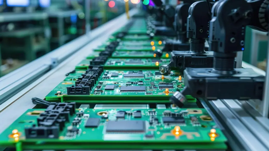
Automated optical inspection system checking PCBs on assembly line
Every AOI machine operates using several inspection techniques:
Pattern recognition to compare component shapes
Color analysis to detect polarity or marking errors
3D profiling to measure solder volume and component height
Rule-based logic to verify spacing, orientation, and placement
These mechanisms enable consistent, high-speed PCB inspection with minimal human intervention.
Interesting Reads: A Step-by-Step Guide to the PCB Assembly Process in Electronic Manufacturing
Components of an AOI Machine
A typical optical inspection system components setup includes:
High-resolution industrial cameras
Precision LED lighting systems
Motion stages for board positioning
Inspection software with comparison algorithms
User interface for operator validation
Together, these elements allow rapid and accurate PCB inspection while minimizing defect escape.
You may also read: Top 10 Essential Printed Circuit Board Components and How Do They Work
AOI Algorithms: From Rules to AI
Earlier AOI systems relied on rigid rule-based programming. Any slight deviation from predefined tolerances triggered an alert, often resulting in excessive false positives.
Modern systems leverage artificial intelligence. AI-driven automated optical inspection learns from historical inspection data, improving accuracy over time. This reduces false calls while enhancing true defect detection rates—making inspection smarter and more efficient.
AOI for Bare PCBs vs Assembled PCBs
Bare board AOI identifies issues such as open circuits, shorts, and damaged traces before component placement.
Assembled board AOI evaluates mounted components, solder joints, orientation, and polarity accuracy.
Implementing AOI systems at both stages ensures comprehensive quality coverage throughout the manufacturing process.
Common Defects Detected by AOI
AOI machines effectively detect:
Missing components
Solder bridges
Lifted leads
Tombstoning
Incorrect orientation
Polarity errors
Cold solder joints
Identifying these defects early prevents downstream failures and improves overall product lifespan.
AOI in High-Speed or Mass Manufacturing
In high-throughput production environments, manual inspection cannot keep pace. Inline AOI systems inspect each board in real time without interrupting workflow.
They provide immediate feedback to engineering teams, allowing process adjustments before defects multiply. This capability is critical for maintaining yield in large-scale PCB assembly operations.
AOI Standards and Industry Compliance
Automated optical inspection supports compliance with:
IPC-A-610
ISO 9001
Aerospace and FDA requirements
Inspection data generated by AOI ensures traceability, documentation, and regulatory readiness.
Limitations of AOI
Despite its advantages, AOI has limitations:
Cannot inspect hidden solder joints
Struggles with highly reflective surfaces
Shadowing from tall components may obscure smaller parts
Requires proper tuning to reduce false positives
For comprehensive inspection, many manufacturers combine PCB AOI with X-ray inspection or in-circuit testing.
Applications of AOI Across Industries

PCB quality inspection testing equipment in electronics lab
AOI systems are widely adopted in:
Automotive systems
Drones and robotics
Telecommunications infrastructure
Aerospace and defense
SMT AOI remains essential in industries where consistent electronics performance and reliability are critical.
Best Practices for AOI Deployment in PCBA
Maximizing AOI performance requires strategic implementation:
Install AOI immediately after reflow
Maintain updated golden board references
Train operators to verify inspection flags
Combine with complementary inspection methods
Schedule regular calibration and maintenance
When properly deployed, automated optical inspection becomes a cornerstone of modern quality control.
Future Trends in AOI
AOI technology continues to evolve rapidly.
Smarter detection algorithms are reducing false calls and improving defect classification accuracy.
System integration allows AOI data to feed directly into ERP and MES platforms for real-time production monitoring.
Remote monitoring enables engineers to review inspection performance from anywhere.
Collaborative robots (cobots) are beginning to work alongside AOI systems for automated defect handling.
Cloud-based reporting supports multi-site manufacturing consistency.
These advancements are transforming AOI systems into intelligent quality management tools.
Conclusion
Automated optical inspection enhances product quality, reduces production costs, and accelerates manufacturing timelines. By detecting defects early, it safeguards reliability and improves overall process efficiency.
As electronic assemblies grow more complex, AOI becomes increasingly critical. It is not merely an inspection tool it is a strategic component of advanced manufacturing.
Frequently Asked Questions
What are 2D and 3D AOI systems?
2D AOI captures surface images to detect visible defects. 3D AOI measures height and solder volume for deeper analysis.
Can AOI replace X-ray inspection?
No. AOI inspects surface-level defects, while X-ray inspection detects hidden internal faults.
How does AOI reduce PCB manufacturing and assembly costs?
By identifying defects early, AOI reduces scrap, minimizes rework, and improves yield efficiency.
Is AOI suitable for small-batch production?
Yes. Offline AOI systems are ideal for prototypes and low-volume runs.
How is AOI evolving with Industry 4.0?
AOI now integrates with smart factory systems, uses AI-based inspection logic, and supports remote monitoring and predictive analytics.
Comment